Silicon photonics chip is to integrate waveguide, modulator, detector, MUX, and DeMUX on silicon platforms by using CMOS semiconductor technology. Compared with the traditional discrete devices, silicon photonics integrated chip is found to be featured with the characteristics of low cost, low energy consumption, high integration, and high transmission bandwidth.
To assemble the silicon photonics integrated chip into an optical transceiver, optical fibers need to be coupled with silicon waveguide. Silicon optical fibers carry an increasing fraction of television programs and Internet traffic. Considering the high integration of Silicon photonics chip, it is better to use a fiber array for chip coupling. Besides, the waveguide of the photonics chip is small, it cannot be coupled with regular single-mode fiber directly. Therefore, some transition processing is needed.
There are vertical coupling and horizontal coupling between the silicon chips and fibers. Some typical coupling schemes of fiber array are introduced here.
In this coupling scheme, the end face of the silicon chip is etched to form a V groove array for placing the fiber array, as shown in Figure. The green cuboid is polymer Lid, which is pressed on the fiber array so the fibers can fall perfectly into the grooves. The position of each fiber can be further adjusted to make the fiber fall into the V-groove completely and achieve the optimal coupling efficiency.
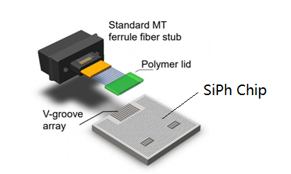
Figure 1
Based on this end-face coupling scheme, Zhongshan MEISU provides fiber arrays of any fiber counts with single-mode fiber, multi-mode fiber, or polarization-maintaining fiber.
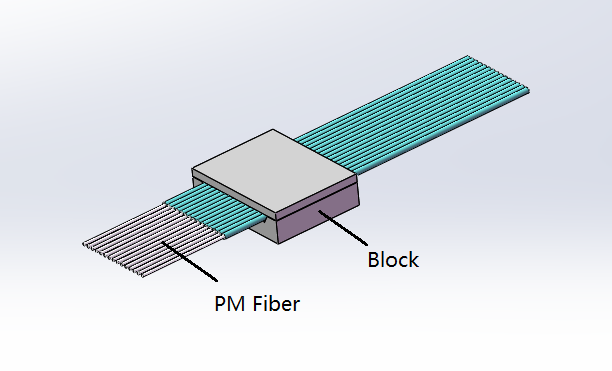
Figure2 PM fiber ribbon
As shown in Figure 3, the polymer waveguide acts as a bridge between the single-mode fiber array and the silicon waveguide. Light is coupled from the single-mode fiber array into the polymer waveguide, which is then coupled into the silicon waveguide.
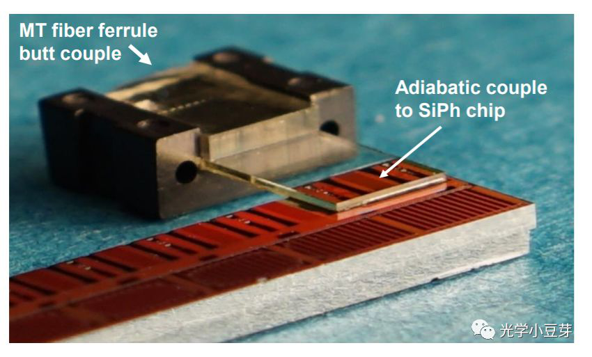
Figure 3 Polymer waveguide coupling
Due to the small waveguide mode field on a silicon chip, ordinary SM fiber coupling will cause a big loss for the mismatching of mode field diameter (MFD). The scheme is to fuse a small section of fiber with small mode field diameter (MFD) to the single-mode fiber array, converting the larger MFD in the fiber to the smaller MFD that can be coupled into the silicon chip. As shown in figure 4, a small mode field fiber acts as an intermediate object equivalent to an Interposer.
Zhongshan MEISU is capable of providing all kinds of MFD matching SM and PM fiber array.
![]()
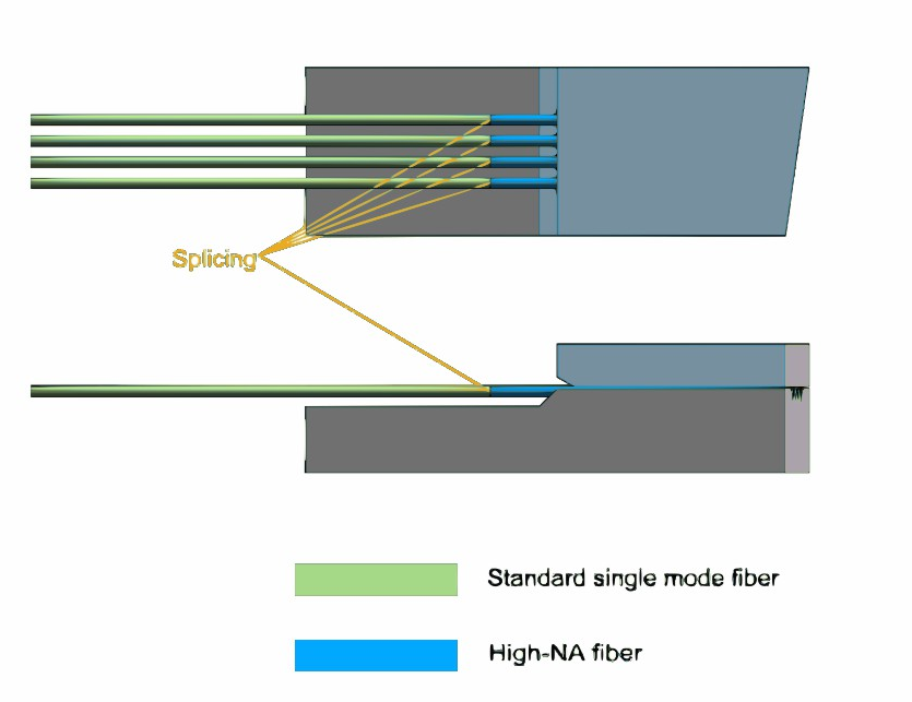
Figure 4 MFD matched Fiber Array
Lensed fiber arrays are an efficient coupling light from photonic integrated chips. Lensed fiber is used for coupling in this scheme. The MFD of Lensed fiber is only about 3um, which can be effectively coupled to the silicon waveguide, as shown in figure 5.
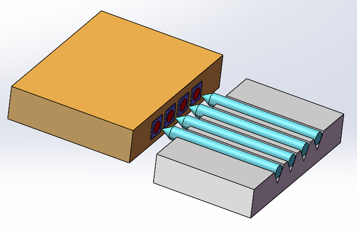
Figure5 lensed fiber array
Zhongshan MEISU offers custom lensed fiber array, the number of channels, fiber spacing, fiber type can be customized according to customer requirements.
First, a vertically coupled waveguide is etched on a photonic chip, and then couple it by using a fiber array with a 45 degrees polished facet to realize vertical coupling in the grating, as shown in figure 6.

Figure6 ![]()
Based on the coupling scheme of 45-degree fiber array, Zhongshan MEISU has developed various types of 45-degree fiber array for different applications, such as 45-degree lidless fiber array, lid recessed fiber array, double layer fiber array, etc.
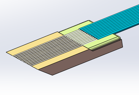
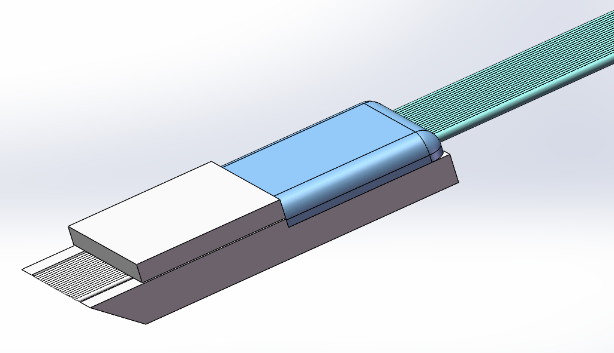
45D Lidless FA 45D Recessed Lid FA
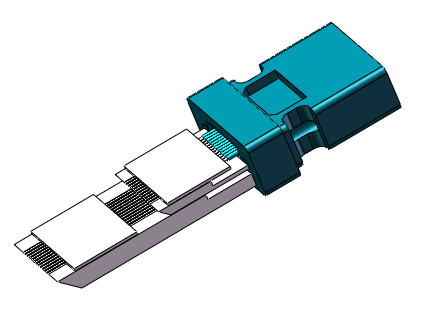
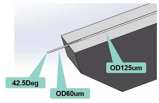
Double-layer 45D FA 45D FA with small fiber diameter
This scheme is a planar coupling scheme, similar to the 45-degree fiber array scheme. The 90-degree fiber array can be easily applied to different positions on silicon optical chip, which is useful for the flexible design of the silicon photonics chip.
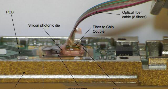
Figure 8 90degree fiber array coupling with PIC chip
Zhongshan Meisu optoelectronics can provide custom 90-degree bending fiber according to customer requirements.
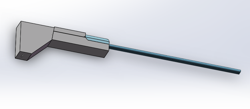
Figure 9 90 degrees fiber array
To meet the different coupling requirements of silicon photonics chips, Zhongshan MEISU developed a variety of small-sized and 260C resistant fiber array for customers over the world.
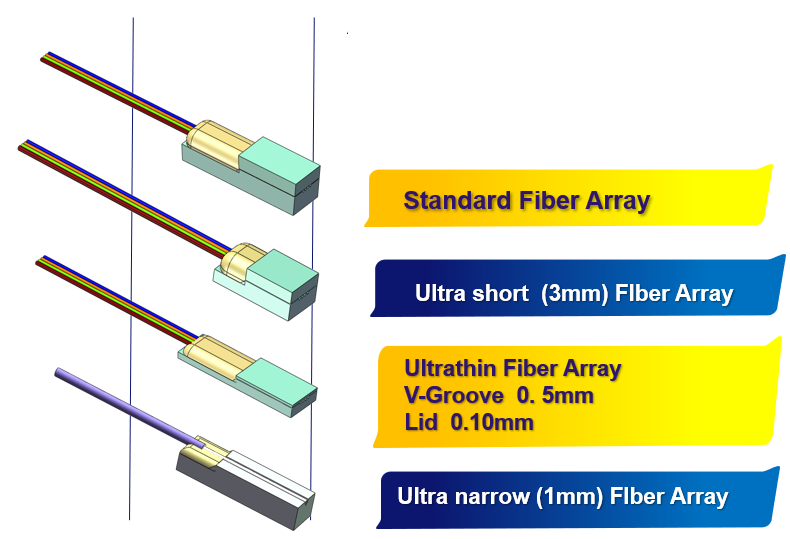
Figure 10 ultra-small fiber array
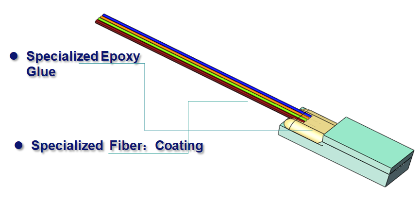
Figure 11 260C resistant fiber array
In general, end face couplers are facing the problem of MFD matching, while grating couplers which require for a specific angle of incident light need to solve the problem of optical path deviation.
For different coupling packaging solutions, Zhongshan MEISU can provide corresponding fiber array products and solutions, and we can also customize various special fiber array according to the specific requirements of customers.
References:
1. P. Fortier, et.al., "Automated High-Throughput Assembly for Photonic Packaging"
2. P.O‘Brien, "Packaging of Integrated Photonic Devices"
3. D. Neugroschl,"Optical Input / Output Considerations for Photonic Integrated Circuit Coupling & Packaging”